Affichage des articles dont le libellé est Electronics(EN). Afficher tous les articles

lundi 7 février 2011

CATHODE RAY OSCILLOSCOPE

The cathode ray oscilloscope [CRO] is an electronic device, which is capable of giving a visual indication of a signal waveform. It is widely used for trouble shooting radio and television receivers as well as laboratory work involving research and design. In addition the oscilloscope can also be used for measuring voltage, frequency and phase shift.

Cathode Ray Tube


A cathode ray tube is the heart of the oscilloscope. It is a vacuum tube of special geometrical shape and converts an electrical signal into visual one. A cathode ray tube makes available plenty of electrons. These electrons are accelerated to high velocity and are brought to focus on a fluorescent screen. The electron beam produces a spot of light wherever it strikes. The electron beam is deflected on its journey in response to the electrical signal under study. The result is that electrical signal waveform is displayed visually.

dimanche 6 février 2011

AM Radio Receiver

In order to reproduce the AM wave into sound waves, every radio receiver must perform the following functions.

1.      The receiving aerial must intercept a portion of the passing radio waves.
2.      The radio receiver must select the desired radio from a number of radio waves intercepted by the receiving aerial. For this purpose tuned parallel LC circuits must be used. These circuits will select only that radio frequency which is resonant with them.
3.      The selected radio wave must be amplified by the tuned frequency amplifiers.
4.      The audio signal must be recovered from the amplified radio wave.
5.      The audio signal must be amplified by suitable number of audio-amplifiers.
6.      The amplified audio signal should be fed to the speaker for sound reproduction.


Types of AM radio receivers


1.      Straight Radio receiver
2.      Superhetrodyne radio receiver

AM diode detector


Fig. below shows a simple diode detector employing a diode and a filter circuit. A detector circuit performs the following two functions.

  1. It rectifies the modulated wave.
  2. It separates the audio signal from the carrier.

  • The modulated wave of desired frequency is selected by the parallel tuned circuit L1C1 and is applied to the diode. During positive half cycles of the modulated wave the diode conducts, while during negative half cycles it doesnot. The result is the output of diode consists of positive half cycle of modulated wave as shown in figure.

  • The rectified output consists of r.f. component and the audio signal which cannot be fed to the speaker for sound reproduction. The r.f. component is filtered  by the capacitor ‘C’ shunted across the speaker. The value of ‘C’ is large enough to present low reactance to the r.f. component . fc+fs  Therefore signal is passed to the speaker.

Frequency modulation

When the frequency of carrier wave is changed in accordance with the intensity of the signal, it is called frequency modulation”.

  • Here the amplitude of the modulated wave remains the same ie carrier wave amplitude.
  • The frequency variations of carrier wave depend upon the instantaneous amplitude of the signal.
  • When the signal approaches positive peaks as the B and F, the carrier frequency is increased to maximum and during negative peak, the carrier frequency is reduced to minimum as shown by widely spaced cycles.

Advantages of FM


  1. It gives noiseless reception.
  2. The operating range is quite large.
  3. The efficiency of transmission is very high.


Demodulation


The process of recovering the audio signal from the modulated wave is known as demodulation or detection.

At the broadcasting station, modulation is done to transmit the audio signal over larger distances. When the modulated wave is picked up the receiver, it is necessary to recover the audio signal from it. This process is accomplished in the radio receiver and is called demodulation.

Transistor AM modulator

  • A circuit which does amplitude modulation is called AM modulator.
  • Fig. above shows the circuit of a simple AM modulator. It is essentially a CE amplifier having a voltage gain of A. The carrier signal is the input  to the amplifier. The modulating signal is applied in the emitter resistance circuit.
  • The amplifier circuit amplifies the carrier by a factor “A” so that the output is Aec. Since the modulating signal is part of the biasing circuit it produces low-frequency variations in the circuit. This in turn causes variations in “A”. The result is that the amplitude of the carrier varies in accordance with the strength of the signal. The amplitude modulated output is obtained across RL.


Power in AM wave


Limitations of Amplitude Modulation


  1. Noisy Reception- In an AM wave, the signal is in the amplitude variations of the carrier. Practically all the natural and man made noises consist of electrical amplitude disturbances. As a radio receiver cannot distinguish between amplitude variations that represent noise and those that contain the desired signal. Therefore reception is very noisy.

  1. Low efficiency- In AM useful power is in the sidebands as they contain the signal. An AM wave has low sideband power.

For example even if modulation is 100 % ie m=1.


PS=33% of PT

Sideband power is only one-third of the total power of AM wave. Hence efficiency of this type of modulation is low.

3- Lack of audio quality- In order to attain high fidelity reception, all audio frequencies upto 15 Khz must be reproduced. This necessitates a bandwidth of 30 KHz since both sidebands must  be reproduced (2fs ). But AM broadcasting stations are assigned with bandwidth of only 10 KHz to minimize the interference from adjacent broadcasting stations. This means that the highest modulating frequency can be 5 Khz which is hardly sufficient to reproduce the music properly.


samedi 5 février 2011

Amplitude modulation

When the amplitude of high frequency carrier wave is changed in accordance with the intensity of the signal, it is called amplitude modulation.

The following points are to be noted in amplitude modulation .
  1. The amplitude of the carrier wave changes according to the intensity of the signal.
  2. The amplitude variations of the carrier wave is at the signal frequency fS.
  3. The frequency of the amplitude modulated wave remains the same ie.carrier frequency fC.

Modulation factor

Radio Broadcasting, Transmission and Reception

Radio communication means the radiation of radio waves by the transmitting station, the propagation of these waves through space and their reception by the radio receiver.

Fig. below shows the general principle of radio broadcasting, transmission and reception. It essentially consists of transmitter, transmission of radio waves and radio receiver.

Transmitter-

It essentially consists of microphone, audio amplifiers, oscillator and modulator.

A microphone is a device which converts sound waves into electrical waves. The output of microphone is fed to multistage audio amplifier for raising the strength of weak signal.

The job of amplification is performed by cascaded audio amplifiers. The amplified output from the last audio amplifier is fed to the modulator for rendering the process of modulation.
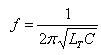
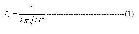
The function of the oscillation is to produce a high frequency signal called a carrier wave. Usually crystal oscillator is used for the purpose.

The amplified audio signal and carrier waves are fed to the modulator. Here the audio signal is superimposed on the carrier wave in suitable manner. The resultant waves are called modulated waves, and the process is called modulation. The process of modulation permits the transmission of audio signal at the carrier signal (frequency). As the carrier frequency is very high, therefore the audio signal can be transmitted to large distances. The radio waves from the transmitter are fed to the transmitting antenna or aerial from where these are radiated into space.

The transmitting antenna radiates the radio waves in space in all directions. These radio waves travel with the velocity of light 3x10⁸m/sec. The radio waves are electromagnetic waves and possess the same general properties.

Receiver-

On reaching the receiving antenna, the radio waves induce tiny emf in it. This small voltage is fed to the radio receiver. Here the radio waves are first amplified and then signal is extracted from them by the process of demodulation. The signal is amplified by audio amplifiers and then fed to the speaker for reproduction into sound waves.

Need for  modulation


1.      Practical Antenna length-theory shows that in order to transmit a wave effectively the length of the transmitting antenna should be approximately equal to the wavelength of the wave.

As the audio frequencies range from 20 Hz to 20Khz, if they are transmitted directly into space, the length of the transmitting antenna required would be extremely large. For example to radiate a frequency of 20 KHz directly into space we would need an antenna length of 3x10⁸ /20x103 ≈ 15,000 meters. This is too long to be constructed practically.

1.      Operating Range- The energy of a wave depends upon its frequency. The greater the frequency of the wave, the greater the energy possessed by it. As the audio signal frequencies are small, therefore these cannot be transmitted over large distances if radiated directly into space.

2.      Wireless communication- Radio transmission should be carried out without wires.


Modulation- The process of changing some characteristics (example amplitude, frequency or phase) of a carrier wave in accordance with the intensity of the signal is known as modulation.

Types of modulation-

  1. Amplitude modulation
  2. Frequency modulation
  3. Phase modulation

Transistor Crystal Oscillator

Figure: Circuit diagram of Transistor crystal oscillator

  • Figure shows the transistor crystal oscillator. The crystal will act as parallel –tuned circuit. At parallel resonance, the impedance of the crystal is maximum. This means that there is a maximum voltage drop across C2. This in turn will allow the maximum energy transfer through the feedback network.

  • The feedback is +ve. A phase shift of 1800 is produced by the transistor. A further phase shift of 1800 is produced by the capacitor voltage divider. This oscillator will oscillate only at fp.

Where fp = parallel resonant frequency ie the frequency at which the vibrating crystal behaves as a parallel resonant circuit.


Advantages


    1. Higher order of frequency stability
    2. The Q-factor of the crystal is very high.

Disadvantages

1.     Can be used in low power circuits.
2.     The frequency of oscillations cannot be changed appreciably.

vendredi 4 février 2011

RC Phase Shift Oscillator

  • It consists of a conventional single transistor amplifier and a RC phase shift circuit. The RC phase shift circuit consists of three sections R1C1, R2C2, and R3C3.At some particular frequency f0 the phase shift in each RC section is 600 so that the total phase shift produced by the RC network is 1800. The frequency of oscillation is given by

  • When the circuit is switched ON it produces oscillations of frequency determined by equation 1. The output EO of the amplifier is feedback to RC feedback network. This network produces a phase shift of 1800 and the transistor gives another 1800 shift. Thereby total phase shift of the output signal when fed back is 3600


Merits-
    1. They do not require any transformer or inductor thereby reduce the cost.
    2. They are quite useful in the low frequency range where tank circuit oscillators   cannot be used.
    3. They provide constant output and good frequency stability.

Demerits –


  1. It is difficult to start oscillations.
  2. The circuit requires a large number of components.
  3. They cannot generate high frequencies and are unstable as variable frequency generators.


Colpitt’s Oscillator

  • The tank circuit is made up of C1, C2  and L. The frequency of oscillations is determined by:

  • When the circuit is turned ON, the capacitor C1 and C2 are charged. The capacitors discharge through L setting up oscillations of frequency determined by expression. 1. The output voltage appears across C2 and feedback voltage is developed across C1. The voltage across C1 is 1800 out of phase with the voltage developed across C2 (Vout ). A phase shift of 1800 is produced by the transistor and a further phase shift of 1800 is produced by C1-C2 voltage divider. In this way feedback is properly phased to produce continuous undamped oscillations.

Feedback factor


Feedback factor


Demerits of Oscillator using Tank Circuit


  1. They suffer for frequency instability and poor waveform
  2. They cannot be used to generate low frequencies, since they become too-much bulky and expensive too.

Hartley Oscillator

The circuit diagram of Hartley Oscillator is as shown in figure below. It uses two inductors placed across common capacitor C and the center of two inductors ins tapped. The tank circuit is made up of L1 , L2 and C and is given by.


 where                LT = L1 + L2 + 2M
         
                           M= Mutual inductance between L1 and L2


  • When the circuit is turned ON, the capacitor is charged. When this capacitor is fully charged, it discharges through coils L1 and L2 setting up oscillations of frequency determined by expression 1. The output voltage of the amplifier appears across L2 and feedback voltage across L1. The voltage across L1 is 1800  out of phase with the voltage developed across L2.
  • A phase shift of 1800 is produced by the transistor and a further phase shift of 1800 is produced by L1-L2 voltage divider circuit. In this way feedback is properly phased to produce continuous undamped oscillations.

Feedback fraction- In Hartley oscillator the feedback voltage is across L1 and output voltage is across L2.

Therefore  feedback fraction

jeudi 3 février 2011

Essentials of Transistor Oscillator

Fig. below shows the block diagram of an oscillator. Its essential components are:

  1. Tank Circuit: It consists of inductance coil(L) connected in parallel with capacitor(C ). The frequency of oscillations in the circuit depends upon the values of inductance of the coil and capacitance of the capacitor.
  2. Transistor Amplifier: The transistor amplifier receives d.c. power from the battery and changes it into a.c. power for supplying to the tank circuit. The oscillations occurring in the tank circuit are applied to the input the transistor amplifer. The output of the transistor can be supplied to the tank circuit to meet the losses.
  3. Feedback circuit: The feedback circuit supplies a part of collector energy to the tank circuit in correct phase to aid the oscillations. ie. provides positive  feedback.


Types of Transistor Oscillators


  1. Hartley Oscillator
  2. Colpitt’s Oscillator
  3. Phase Shift Oscillator
  4. Tuned Collector Oscillator
  5. Wein Bridge Oscillator
  6. Crystal Oscillator

Undamped Oscillations from Tank Circuit

A tank circuit produces damped oscillations. In practice we need continuous undamped oscillations for the successful operation of electronics equipment. In order to make the oscillations in the tank circuit undamped it is necessary to supply correct amount of energy to the tank circuit at the proper time intervals to meet the losses.


The following conditions must be fulfilled;

1.      The amount of energy supplied be such so as to meet the losses in the tank and the a.c. energy removed from the circuit by the load. For example if losses in LC circuit amount ot 5 mW and a.c. output being taken is 100 mW, then power of 105mW should be continuously supplied to the circuit.
  1. The applied energy should have the same frequency as the of the oscillations in the tank circuit.
  2. The applied energy should be in phase with the oscillations set up in the tank circuit.

Positive feedback Amplifier-Oscillator


  1. A transistor amplifier with proper +ve feedback can act as an oscillator.


  1. The circuit needs only a quick trigger signal to start the oscillations. Once the oscillations have started, no external signal source is necessary.
  2. In order to get continuous undamped output from the circuit, the following condition must be met;
             mvAV =1
          where AV = voltage gain of amplifier without feedback.
                     mv = feedback fraction.
        This relation is also called Barkhausen criterion

Types of Sinusoidal Oscillations

  1. Damped Oscillations
  2. Undamped Oscillations

  1. Damped Oscillations-The electrical oscillations whose amplitude goes on decreasing with time are called damped oscillations.
  2. Undamped Oscillations- The electrical oscillations whose amplitude remains constant with time are called undamped oscillations.

Oscillatory circuit

A circuit, which produces electrical oscillations of any desired frequency, is known as an oscillatory circuit or tank circuit.

A simple oscillatory circuit consists of a capacitor C and inductance coil L in parallel as shown in figure below. This electrical system can produce electrical oscillations of frequency determined by the values of L and C.


Circuit operations- Assume capacitor is charged from a d. c. source with a polarity as shown in figure 1.

  • When switch S is closed as shown in fig.ii, the capacitor will discharge through inductance and the electron flow will be in the direction indicated by the arrow. This current flow sets up magnetic field around the coil. Due to the inductive effect, the current builds up slowly towards a maximum value. The circuit current will be maximum when the capacitor is fully discharged. Hence the electrostatic energy across the capacitor is completely converted into magnetic field energy around the coil.
  • Once the capacitor is discharged, the magnetic field will begin to collapse and produce a counter emf. According to Lenz’s law the counter emf will keep the current flowing in the same direction. The result is that the capacitor is now charged with opposite polarity making upper plate of capacitor –ve and lower plate +ve as shown in fig. 3.
  • After the collapsing field has recharged the capacitor, the capacitor now begins to discharge and current now flows in the opposite direction as shown in fig. iv.
  • The sequence of charge and discharge results in alternating motion of electrons or an oscillating current. The energy is alternately stored in the lectric field of the capacitor C and the magnetic field of the inductance coil L . This interchange of energy between L and C is repeated over and again resulting in the production of Oscillations.

Waveform- In practical tank circuit there are resistive and radiation losses in the coil and dielectric losses in the capacitor. During each cycle a small part of the originally imparted energy is used up to overcome these losses. The result is that the amplitude of oscillating current decreases gradually and eventually it become zero. Therefore tank circuit produces damped oscillations.

Frequency of oscillations- The expression for frequency of oscillation is given by,


mercredi 2 février 2011

Applications of Op-Amp

Applications of Op-Amp


An Op-Amp can be used as
  1. Inverting Amplifer
  2. Non-Iverting Amplifer
  3. Voltage follower
  4. Adder ( Summer)
  5. Integrator
  6. Differentiator


Definitions

Slewrate(S): It is defined as “ The rate of change of output voltage per unit time”


OPERATIONAL AMPLIFEIR

INTRODUCTION

Op-Amp (operational amplifier) is basically an amplifier available in the IC form. The word “operational” is used because the amplifier can be used to perform a variety of mathematical operations such as addition, subtraction, integration, differentiation etc.

Figure 1 below shows the symbol of an Op-Amp.


It has two inputs and one output. The input marked “-“  is known as Inverting input and the input marked “+” is known as Non-inverting input.

mardi 1 février 2011

DC Load Line and Operating point selection

Consisder a CE amplifier along with the output characteristics as shown in figure 3.18 above. A straight line drawn on the output characteristic of a transistor which gives the various zero signal values (ie. When no signal applied) of VCE and IC is called DC load line.

Construction of DC load line

Applying KVL to the collector circuit we get,

VCC –ICRC –VCE =0-------------------1

VCE  = VCC –ICRC ----------------------2

The above equation is the first degree equation and can be represented by a straight line. This straight line is DC load line.


To draw the load line we require two end points which can be found as follows.

1.      If IC =0, equn 2 becomes VCE  = VCC
2.      if VCE = 0, equn 2 becomes VCC = ICRC   ie. IC = VCC /RC


3.14 Operating point (Q)

A point on the d.c. load line which represent the zero signal values of VCE and IC in a transistor is called as operating point or silent point or quiescent point or Q-point.

The Q-point is selected where the DC load line intersects the curve of output characteristics for particular value of zero signal current.
  
          i.e. Q-point = (VCE ,IC)

Cascading transistor amplifiers

When the amplification provided by a single stage amplifier is not  suffiecient for a particular purpose or when the input and output impedance is not of the correct magnituded for the required application then two or more amplifiers are connected in
 cascade as shown below.
             
Here the output of amplifier 1 is connected as the input of amplifier 2.

Example: The gain of a single amplifier is not sufficient to amplify a signal from a weak source such as microphone to a level which is suitablefor the operation of another circuit as loud speaker. In such cases, amplifiers are used.

Transistor as an amplifier

Consider a npn transistor in CE configuration as shown above along with its input characteristics.

A transistor raises the strength of a weak input signal and thus acts as an amplifier. The weak signal to be amplified is applied between emitter and base and the output is taken across the load resistor RC connected in the collector circuit.

In order to use a transistor as an amplifier it should be operated in active region i.e. emitter junction should be always FB and collector junction should be RB. Therefore in addition to the a.c. input source Vi two d.c. voltages VEB and VCE are applied as shown. This d.c. voltage is called bias voltage.

As the input circuit has low resistance, a small change in te signal voltage Vi causes a large change in the base current thereby causing the same change in collector current (because IC = βIB).

The collector current flowing through a high load resistance RC produces a large voltage across it. Thus a weak signal applied at the input circuit appears in the amplified form at the output. In this way transistor acts as an amplifier.

Example: Let RC = 5KΩ, Vin =1V, IC =1mA then output V=ICRC =5V


Bias stabilization


The process of making operating point independent of temperature changes or variation in transistor parameters is called the stabilization.

We know that for transistor to operate it should be properly biased so that we can have a fixed operating point. To avoid any distortions, the Q-point should be at the center of the load line.

But in practice this Q-point may shift to any operating region (saturation or cur-off region) making the transistor unstable. Therefore in order to avoid this, biasing stability should be maintained.

Causes for Bias instability


Bias instability occurs mainly due to two reasons.
  1. Temperature
  2. Current gain

1. Temperature (T)

The temperature at the junctions of a transistor depends on the amount of current flowing through it. Due to increase in temperature following parameters of a  transistor will change.

(a)base-emitter voltage (VBE)

VBE increases at a rate of 2.4mV/0C. With increase in temperature the base current IB will increase and since IC= βIB, IC is also increased hence, changing the Q-point.

(b) Reverse saturation current ( ICBO)

We know that IC = βIB + (1+β) ICBO where ICBO is the reverse saturation current. As the temperature increases ICBO increases there by increase in IC and hence changing the Q-point.

2. Current gain (β)

In the process of manufacturing the transistors different transistors of same type may have different parameters ( i.e. if we take two transistor units of same type and use them in the circuit there is a change in the β value in actual practice ). The biasing circuit will be designed according to the required β value but due to the change in β from unit to unit the operating point may shift.

lundi 31 janvier 2011

Transistor configuration

We know that, transistor can be used as an amplifier. For an amplifier, two terminals are required to supply the weak signal and two terminals to collect the amplified signal. Thus four terminals are required but a transistor is said to have only three terminals Therefore, one terminal is used common for both input and output.

This gives rise to three different combinations.
1.      Common base configuration (CB)
2.      Common emitter configuration (CE)
3.      Common collector configuration (CC)

1. CB configuration


A simple circuit arrangement of CB configuration for pnp transistor is shown below.

In this configuration, base is used as common to both input and output. It can be noted that the i/p  section has an a.c. source Vi along with the d.c. source VEB. The purpose of including VEB is to keep EB junction always forward biased (because if there is no VEB then the EB junction is forward biased only during the +ve half-cycle of the i/p and reverse biased during the –ve half cycle). In CB configuration, IE –i/p current, IC –o/p current.